This set of Basic Electronics Engineering Multiple Choice Questions & Answers (MCQs) focuses on “Junction Diode – Zener Diode”.
1. Zener diode is a _______ conducting device.
a) Unidirectional
b) Bidirectional
c) Multidirectional
d) Tri-directional
View Answer
Explanation: A Zener diode is a device which can also allow current to flow in reverse direction, unlike a normal diode. Also, it can allow current to flow current from anode to cathode too. It requires a specific value of voltage so that it can allow reverse current flow which is called as Zener Voltage.
2. What is specifically reduced in a Zener diode compared to a normal diode, which has almost the same properties?
a) Threshold Voltage
b) Knee Voltage
c) Breakdown Voltage
d) Operating Voltage
View Answer
Explanation: The Zener diode has same properties and characteristics as of a normal diode. For example, the minimum forward bias voltage required is 0.3 or 0.7 Volts. But, the special design of Zener diode i.e. heavily doped semiconductor allows it to have a reduced breakdown voltage which is less than that of a normal one.
3. Zener diode in reverse bias state has a controlled breakdown that allows current to keep the voltage close to which of the following?
a) Conduction voltage
b) Knee voltage
c) Threshold voltage
d) Zener breakdown voltage
View Answer
Explanation: When the Zener diode is in reverse biased state, it can undergo breakdown after a specific value of voltage. After going into breakdown, for some values, the voltage level for different current level is same. This voltage level is a controlled one and referred as Zener breakdown voltage.
4. Which one of the below, is defined as the sudden increase in reverse current and generation of carriers rapidly?
a) Field effect
b) Thermal effect
c) Zener effect
d) Transition effect
View Answer
Explanation: The Zener diode is a heavily doped diode due to which it forms a high width depletion layer when an external source is applied. When used in reverse biased state, the value of current is minimum up to a certain point of voltage. This value of voltage generates carriers rapidly in the semiconductors. After the breakdown, there is a sudden increase in reverse current. This effect is called as Zener effect.
5. After how many volts in a silicon-based Zener diode, avalanche breakdown can occur?
a) 5.6
b) 3.4
c) 10
d) 2.2
View Answer
Explanation: Avalanche breakdown occurs, when a tremendous amount of heat is generated. This can destroy the diode if not protected. The cause of heat generated is, due to high value of current passed by the Zener diode. This also produces hysteresis effect on the Zener diode.
6. What is the main reason for the Avalanche breakdown?
a) Magnetic field
b) Electric field
c) Heat
d) Current
View Answer
Explanation: The Avalanche effect or termed as Avalanche breakdown occurs, when a high value current passes through it. This high value of reverse current produces heat and causes hysteresis effect on the Zener diode. After which, suddenly Zener Diode undergoes breakdown and a high drop of voltage is observed.
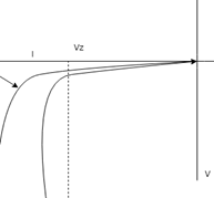
7. In the figure shown below, for a Zener diode the arrow points towards, which of the following?
a) Zener breakdown
b) Avalanche breakdown
c) Reverse breakdown
d) Forward Knee voltage
View Answer
Explanation: In the figure we can observe that there are two breakdowns. Also it indicates the reverse biased I-V characteristics of the Zener diode. The first breakdown is the Zener breakdown, whereas the second one is the Avalanche breakdown. Both the breakdown’s occur simultaneously.
8. For a doped junction, when will the Zener breakdown occur?
a) Heavily doped
b) Light doped
c) Moderately doped
d) Not doped
View Answer
Explanation: Zener effect occurs when a heavily doped semiconductor diode is reverse biased and an external voltage source is supplied. The depletion layer is thick, than compared to the normal diode. The external voltage is generated rapidly and this suddenly increases the reverse current, which causes breakdown.
9. Which of the below is widely used, in the application of Zener diodes?
a) Series regulator
b) Shunt regulator
c) Clamper
d) Rectifiers
View Answer
Explanation: Zener diodes have controlled breakdowns and also the voltage drop after the breakdown is close to the breakdown voltage even if the magnitude of current changes. From this we can conclude that, Zener diodes can be used for constant voltage requirement i.e. regulation of the voltage. Hence it is used as a Shunt regulator, whereas, normal diodes are used in rectifiers and in clamping circuits.
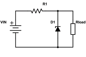
10. If the input voltage is 5 volts and load voltage is 3 volts, resistance R1 as 4Ω, then what will be the diode current for the circuit in the fi below figure?
a) 0.1 A
b) 0.2 A
c) 1.2 A
d) 0.5 A
View Answer
Explanation: From the given figure we can say that,
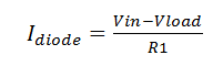
i.e. I = diode current, Vin = 5 Volts, Vload = 3 Volts, R1= 4Ω.
Therefore, I = (5-3)/4 = 0.5 amperes.
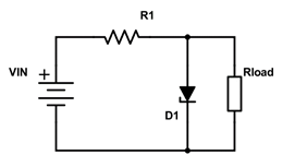
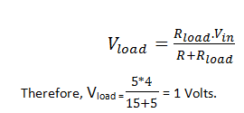
11. If the load resistance is 5Ω, R1= 15Ω, input voltage is 4 Volts, then what will be the load voltage?
a) 2 Volts
b) 3 Volts
c) 1 Volts
d) 1.5 Volts
View Answer
Explanation: From the given figure we can say that,
12. At room temperature, what will be the leakage current of Zener diode?
a) 1µ Ampere
b) 1m Ampere
c) 1n Ampere
d) 1 Ampere
View Answer
Explanation: When a Zener diode is in reversed biased state and is an open circuit, a small amount of current flows into it. This small amount of current is due to the carriers and such current exists until the equilibrium is reached in depletion layer. This small amount current is called as Leakage Current.
Sanfoundry Global Education & Learning Series – Basic Electronics Engineering.
To practice all areas of Basic Electronics Engineering, here is complete set of 1000+ Multiple Choice Questions and Answers.
If you find a mistake in question / option / answer, kindly take a screenshot and email to [email protected]
