This set of Microelectronics Multiple Choice Questions & Answers (MCQs) focuses on “Bipolar Differential Amplifiers – Set 2”.
1. What is the small signal gain for Q1 in the following circuit? Assume that both channel length modulation and early effect is present, only in Q1. The MOSFETs are identical to each other and the Bipolar transistors are identical to each other.
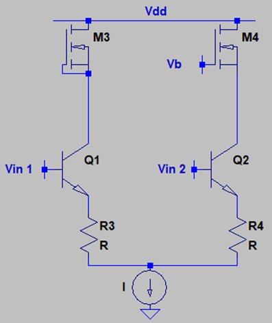
a) –[(gm1/1+(gm1*((R3+R4+1/gm2)||ro1)*(ro1+(1+gm1*ro1) * ((R3+R4+1/gm2)||rπ1)||(ro3||1/gm3)))
b) –[(gm1/1+(gm1*(R3+R4+1/gm2)*(ro1+(1+gm1*ro1)||ro1*((R3+R4+1/gm2)||rπ1)||(ro3||1/gm3)))
c) –[(gm1/1+(gm1*(R3+R4+1/gm2)||ro1*(ro1+(1+gm1*ro1) * ((R3+R4+1/gm2)||rπ1)||(ro3||1/gm3)))
d) –[(gm1/1+(gm1*(R3+R4+1/gm2)||ro1)*(ro1+(1+gm1*ro1) * ((R3+R4+1/gm2)||rπ1)||(ro3||1/gm3)))
View Answer
Explanation: We note that the small signal gain for Q1 has to be analyzed by turning off all voltage sources and current sources. We note that the emitter of Q1 is connected to R3 which is in series with R4 & the resistance looking into the emitter of Q2 in presence of early effect. Henceforth, the total resistance comes connected at the emitter which will affect the transconductance, and the output resistance. The transconductance becomes gm1/1+(gm1*((R3+R4+1/gm2)||ro1)) and the output resistance becomes (ro1+(1+gm1*ro1)*((R3+R4+1/gm2)||rπ1)||(ro3||1/gm3))). Noting that the voltage gain will be for a degenerated CE stage, we can write the voltage gain as –[(gm1/1+(gm1*(R3+R4+1/gm2)||ro1)*(ro1+(1+gm1*ro1)*((R3+R4+1/gm2)||rπ1)||(ro3||1/gm3))).
2. What is the differential voltage gain of the following circuit? Assume that both channel length modulation and early effect is present, the MOSFETs are identical to each other and the Bipolar transistors are identical to each other.
a) –[(gm1/1+(gm1*(R3+ro1)*(ro1+(gm1*ro1)*(R3+rπ1)||(ro3||1/gm3)))+(gm2/1+(gm2*(R4||ro2)*(ro2+(1-gm1*ro1)*(R3||rπ2)||(ro4)))]
b) [(gm1/1+(gm1*(R3+ro1)*(ro1+(gm1*ro1)*(R3+rπ1)||(ro3||1/gm3)))+(gm2/1+(gm2*(R4)*(ro2+(1-gm1*ro1)*(R3||rπ2)||(ro4)))]/2
c) -[(gm1/1+(gm1*((R3+R4+(1/gm2||ro2))||ro1) *(ro1+(1+gm1*ro1) * ((R3+R4+(1/gm2||ro2))||rπ1)||(ro3||1/gm3)))+(gm2/1+(gm2*(R4+(1/gm1||ro1)+R3)||ro2)*(ro2+(1+gm1*ro1)*((R4+(1/gm1||ro1)+R3)||rπ2)||(ro4)))]
d) [(gm1/1+(gm1*(R3+ro1)*(ro1+(gm1*ro1)*(R3+rπ1)||(ro3||1/gm3)))+(gm2/1+(gm2*(ro2)*(ro2-(1+gm1*ro1)*(R3||rπ2)||(ro4)))]/2
View Answer
Explanation: It is evident that the differential voltage gain is the difference between the voltage gain of each transistor. The input to each transistor is different with a phase of 180⁰. The voltage gain for Q1 is –[(gm1/1+(gm1*(R3+R4+(1/gm2||ro2))||ro1)*(ro1+(1+gm1*ro1)*((R3+R4+(1/gm2||ro2))||rπ1)||(ro3||1/gm3)). The voltage gain for Q2 is –(gm2/1+(gm2*(R4+R3+(1/gm1||ro1)||ro2)*(ro2+(1+gm1*ro1)*(R4+R3+(1/gm1||ro1)||rπ2)||(ro4))). The differential voltage gain will be the difference between the voltage gain of \(\frac {(V_{OUT2} – V_{OUT1})}{ (V_{IN2}-V_{IN1})} = \frac { \{ V_{IN}*A_{V2} – (-V_{IN}*A_{v1}) \} }{(V_{IN}-(-V_{IN})}= \frac {(A_{V2}+A_{V1})}{2}\). Note that both the voltage gains are negative and the overall voltage gain will also have a minus sign. We have approximated 1/rπ>>gm. Note that the transconductance doesn’t get affect by the resistance looking from the drain terminal towards the power supply since the drain resistance typically controls the drain voltage.
3. What is the transconductance of Q1 if VA=2V, the collector current is 1mA, R3 = R4 = 1kΩ and the temperature is 300K.
a) gm1/1+(gm1*((1/gm2)||ro1))
b) gm1/1+(gm1*((R3+1/gm2)||ro1))
c) gm1/1+(gm1*(R4+1/gm2||ro1))
d) gm1/1+(gm1*((R3+R4+1/gm2)||ro1))
View Answer
Explanation: We note that Q1 is degenerated by R3 and its transconductance has decreased but the linearity of the circuit will be enhanced. The new transconductance is gm1/1+(gm1*((R3+R4+1/gm2)||ro1)) where gm1 is the transconductance without degeneration.
4. What is the voltage gain of M1? Assume that early effect is absent but channel length modulation is present.
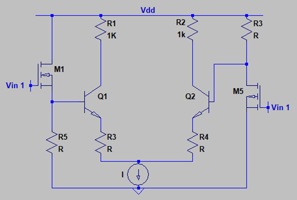
a) rπ+(β+1)*(R3+R4+1/gm+(R3||ro))/(1/gm+(rπ+(β+1)*(R3+R4(R3||ro)/(β+1)))
b) rπ+(β+1)*(R3+R4+(R3||ro)/(β+1))/(1/gm+(rπ+(β+1)*(R3+1/gm+(R3||ro)/(β+1)))
c) rπ+(β+1)*(R3+R4+1/gm+(R3||ro)/(β+1))/(1/gm+(rπ+(β+1)*(R4+1/gm+(R3||ro)/(β+1)))
d) rπ+(β+1)*(R3+R4+1/gm+(R3||ro)/(β+1))/(1/gm+(rπ+(β+1)*(R3+R4+1/gm+(R3||ro)/(β+1)))
View Answer
Explanation: M1 behaves as a source follower so we know that its voltage gain is Rs/(1/gm+Rs). Now, RS is the impedance looking into the base of the transistor which is rπ+(β+1)*RE & RE is R3+R4+1/gm+RB(Q2)/(β+1). We note that RB is simply R3||ro and the overall voltage gain of M1 becomes rπ+(β+1)*(R3+R4+1/gm2+(R3||ro5)/(β+1))/(1/gm+(rπ1+(β+1)*(R3+R4+1/gm2+(R3||ro5)/(β+1)))
5. What is the voltage gain of M5? Assume that early effect is absent but channel length modulation is present.
a) rπ+(β+1)*(R3+R4+1/gm1)||R3||ro5
b) rπ+(β+1)*(R3+R4+(R5||ro1))||R3||ro5
c) rπ+(β+1)*(R3+R4+1/gm1+(R5||ro1)/(β+1))||R3||ro5
d) rπ+(β+1)*(R3+R4+1/gm1+(R5||ro1)/(β+1))||ro5
View Answer
Explanation: M5 is behaving as a CS stage. The voltage gain is RC || ro. RC is connected to the base of Q2 which has an input resistance of rπ+(β+1)*RE. Now, RE is R3+R4+1/gm+RB(Q1)/(β+1). We note that RB is simply R5||ro which is the resistance connected to the source of the M1. Moreover, R3 is also connected to the drain of M5 & the overall voltage gain becomes rπ+(β+1)*(R3+R4+1/gm1+(R5||ro1)/(β+1))||R3||ro5.
6. What is the voltage gain from the gate of M5 to the collector of Q2? Assume channel length modulation is present but early effect is absent.
a) -(rπ+(β+1)*(R3+R4+1/gm1+(R5||ro1)/(β+1))||R3||ro5)*(R2/((R4+R3+1/gm1+R5||ro/(β+1))+1/gm+(R3||ro5)/(β+1)
b) -(rπ+(β+1)*(R3+R4+1/gm1+(R5||ro1)/(β+1))*(R2/((R4+R3+1/gm1+R5||ro/(β+1))+1/gm+(R3||ro5))
c) (rπ+(β+1)*(R5||ro1)/(β+1))||R3||ro5)*(R2/((R4+R3+1/gm1+R5||ro/(β+1))+1/gm+(R3)/(β+1)
d) (rπ+R3+R4+1/gm1+(R5||ro1)/(β+1))||R3||ro5)*(R2/((R4+R3+1/gm1+R5||ro/(β+1))+1/gm+(ro5)/(β+1)
View Answer
Explanation: The voltage gain is a product of the voltage gain of M5, behaving as a CS stage, and that of Q2, behaving as a CE stage. The voltage gain of Q2 is R2/(RE+1/gm+RB/(β+1). Now, RE is R4+R3+1/gm1+R5||ro/(β+1) while RB is R3||ro5. Hence, the voltage gain of only Q2 is R2/((R4+R3+1/gm1+R5||ro/(β+1))+1/gm+(R3||ro5)/(β+1). The voltage gain of M5 is -(rπ+(β+1)*(R3+R4+1/gm1+(R5||ro1)/(β+1))||R3||ro5). The overall voltage gain is -(rπ+(β+1)*(R3+R4+1/gm1+(R5||ro1)/(β+1))||R3||ro5)*(R2/((R4+R3+1/gm1+R5||ro/(β+1))+1/gm+(R3||ro5)/(β+1).
7. What is the voltage gain from the gate of M1 to the collector of Q1? Assume channel length modulation is present but early effect is absent.
a) (rπ+(β+1)*(R3+R4+1/gm+(R3||ro)/(β+1))/(1/gm+(rπ+(β+1)*(R3+R4+1/gm+(R3||ro)/(β+1))))*(R2*(1/gm+(R5||ro5)/(β+1))
b) (rπ+(β+1)*(R3+R4+1/gm+(R3||ro)/(β+1))/(1/gm+(rπ+(β+1) * (R3+R4+1/gm+(R3||ro)/(β+1))))*(R2/((R3+R4+1/gm2+R3||ro/(β+1))+1/gm+(R5||ro5)/(β+1))
c) (rπ+(β+1)*(R3+R4+1/gm+(R3||ro)/(β+1))/(1/gm+(rπ+(β+1)*(R3+R4+1/gm+(R3||ro)/(β+1))))*(R2/((1/gm2+R3||ro/(β+1))+1/gm+(R5||ro5)/(β+1))
d) ((β+1)*(R3+(R3||ro)/(β+1))/(1/gm+(rπ+(β+1)*(R3+R4+1/gm+(R3||ro)/(β+1))))*(R2/((R3+R4+1/gm2+R3||ro/(β+1))+1/gm+(R5||ro5)/(β+1))
View Answer
Explanation: We note that the voltage gain is a product of the voltage gain of M1 & the voltage gain of Q1. The voltage gain of only Q1 is R1/(RE+1/gm+RB/(β+1). Now, RE is R3+R4+1/gm2+R3||ro/(β+1) while RB is R5||ro5. Hence, the voltage gain of only Q2 is (R2/((R3+R4+1/gm2+R3||ro/(β+1))+1/gm+(R5||ro5)/(β+1)). The voltage gain of M1 is rπ+(β+1)*(R3+R4+1/gm+(R3||ro)/(β+1))/(1/gm+(rπ+(β+1)*(R3+ R4+1/gm+(R3||ro)/(β+1))). The overall voltage gain is (rπ+(β+1)*(R3+R4+1/gm+(R3||ro)/(β+1))/(1/gm+(rπ+(β+1)*(R3+ R4+1/gm+(R3||ro)/(β+1))))*(R2/((R3+R4+1/gm2+R3||ro/(β+1))+1/gm+(R5||ro5)/(β+1)).
8. What is the total output impedance of Q1? Assume that both channel length modulation and early effect is present, the MOSFETs are identical to each other and the Bipolar transistors are identical to each other.
a) ro1+(1+ro1)((R4+R3+(1/gm||ro))||rπ1)||(ro3+1/gm3)
b) ro1+(1+gm1*ro1)(rπ1)||(ro3+1/gm3)
c) ro1+(1+gm1*ro1)((R4+R3+(1/gm||ro))||rπ)||(ro3+1/gm3)
d) r01q+(1+gm1*ro1)(R3)||(ro3+1/gm3)
View Answer
Explanation: We note that Q1 is degenerated by R3 and hence, the output impedance looking into the collector of the NPN transistor is ro+(1+gm*ro)(R3||rπ). We also note that M3, behaving as a diode-connected device, offers a resistance of (ro3+1/gm3), looking into it’s drain terminal, and the drain is connected to the collector of Q1. We remember that these resistances are small signal values and the are all connected from the collector terminal to ground, since VDD is grounded during small signal analysis and the current source is made open. The overall resistance becomes ro+(1+gm*ro)(R3||rπ)||(ro3+1/gm3).
9. What is the total output impedance of Q2? Assume that both channel length modulation and early effect is present, the MOSFETs are identical to each other and the Bipolar transistors are identical to each other.
a) ro2+(1+ro2)(R3||rπ2)||(ro3+1/gm3)
b) ro2+(1+gm2+ro2)(rπ2)||(ro4)
c) ro2+(1+gm2+ro2)((R4+R3+(1/gm||ro))||rπ2)||(ro4)
d) ro2+(1+gm2+ro2)((R4+R3+(1/gm||ro)))(R3)||(ro3+1/gm3)
View Answer
Explanation: We note that Q1 is degenerated by R3 and hence, the output impedance looking into the collector of the NPN transistor is ro+(1+gm*ro)(R3||rπ). We also note that M3, behaving as a diode-connected device, offers a resistance of (ro3||1/gm3), looking into it’s drain terminal, and the drain is connected to the collector of Q1. We remember that these resistances are small signal values and the are all connected from the collector terminal to ground, since VDD is grounded during small signal analysis and the current source is made open. The overall resistance becomes ro2+(1+gm2+ro2)(R3||rπ2)||(ro4).
10. What is the output at the collector of Q1 due to VIN1 at M5? Note that early effect is absent but channel length modulation is present.
a) R3*RC/(1/gm+(R4+1/gm2+R3||ro/(β+1)))
b. [(rπ+(β+1)*(R3+R4+1/gm1+(R5||ro1)/(β+1))||R3||ro)]*RC/(1/gm+ (R3+R4+1/gm2+R3||ro/(β+1)))
c) RC/(1/gm+ (R3+R3||ro/(β+1)))
d. [(rπ+(β+1)*(R3+R4+1/gm1+(R5||ro1)/(β+1))||R3||ro)]*RC/(1/gm+ (R3+R3||ro/(β+1)))
View Answer
Explanation: For VIN1 at M1, the output at Q1 is the gain for a CB stage. A C.B. stage shows a voltage gain of RC/(1/gm+RE) & RE is the resistance connected to the emitter of Q1 which is R3+R4+1/gm2+R3||ro/(β+1). The overall voltage gain becomes the product of the voltage gain of M5 as a CS stage and RC/(1/gm+(R3+R4+1/gm2+R3||ro/(β+1))) i.e. [(rπ+(β+1)*(R3+R4+1/gm1+(R5||ro1)/(β+1))||R3||ro)]*RC/(1/gm+ (R3+R4+1/gm2+R3||ro/(β+1))).
11. What is the output at the collector of Q2 due to VIN1 at M1? Note that early effect is absent but channel length modulation is present.
a) (rπ+(β+1)*(R3+R4+1/gm+(R3||ro)/(β+1))/(1/gm+(rπ+(β+1)*(R3+R4+1/gm+(R3||ro)/(β+1))))*RC/(1/gm+ (R3+R4+1/gm2+R3||ro/(β+1)))
b) (rπ+(β+1)*(R3+R4+1/gm+(R3||ro)/(β+1))/(1/gm+(rπ+(β+1)*(R3+R4+1/gm+(R3||ro)/(β+1))))*RC/( (R3+R4+R3||ro/(β+1)))
c) (rπ+(R3+R4+1/gm+1/(β+1))/(1/gm+((R3+R4+1/gm+(R3||ro)/(β+1))))*RC/(1/gm+ (R3+R4+1/gm2+R3||ro/(β+1)))
d) (rπ+(β+1)*(R3+R4+1/gm+(R3||ro)/(β+1))/(1/gm+(rπ+(β+1)*(R3+R4+1/gm+(R3||ro)/(β+1))))*RC/(1/gm+ (R3+R4+1/gm1+R5||ro/(β+1)))
View Answer
Explanation: For VIN1 at M1, the output at collector of Q2 is the gain for a CB stage. A C.B. stage shows a voltage gain of RC/(1/gm+RE) & RE is the resistance connected to the emitter of Q2 which is R4+R3+1/gm1+R5||ro/(β+1). The overall voltage gain becomes the product of the voltage gain of M1 as a follower stage and RC/(1/gm2+ (R4+R3+1/gm1+R5||ro/(β+1))) ie (rπ+(β+1)*(R3+R4+1/gm+(R3||ro)/(β+1))/(1/gm+(rπ+(β+1)*(R3+R4+1/gm+(R3||ro)/(β+1))))*RC/(1/gm+ (R4+R3+1/gm1+R5||ro/(β+1))).
12. What is the output at the collector of Q1 due to VIN1 at both M1 & M2? Note that early effect is absent but channel length modulation is present. Assume that all are identical and working in the linear region of operation.
a) [(rπ+(β+1)*(R3+R4+1/gm+(R3||ro)/(β+1))/(1/gm+(rπ+(β+1) * (R3+R4+1/gm+(R3||ro)/(β+1))))*(R2/((R3+R4+1/gm2+R3||ro/(β+1))+1/gm+(R5||ro5)/(β+1))]+[[(rπ+(β+1)*(R1||ro)]*RC/(1/gm+(R3+R4+1/gm2+R3||ro/(β+1)))]
b) [(rπ+(β+1)*(R3+R4+1/gm+(R3||ro)/(β+1))/(1/gm+(rπ+(β+1)*(R3+R4+1/gm+(R3||ro)/(β+1)))) *(R2/((R3+R4+1/gm2+R3||ro/(β+1))+1/gm+(R5||ro5)/(β+1))]+[[(rπ+(β+1) * (R3+R4+1/gm1+(R5||ro1)/(β+1))||R3||ro)] * RC/(1/gm+(R3+R4+1/gm2+R3||ro/(β+1)))]
c) [(rπ+(β+1)*(R3+R4+1/gm+(R3||ro)/(β+1))/(1/gm+(rπ+(β+1) * (R3+R4+1/gm+(R3||ro)/(β+1)))) *(R2/((1/gm2+R3||ro/(β+1))+1/gm+(R5||ro5)/(β+1))]+[[(rπ+(β+1) * (R3+R4+1/gm1+(R5||ro1)/(β+1))||R3||ro)]
d) [((β+1)*(R3+R4+1/gm+(R3||ro)/(β+1))/(1/gm+(rπ+(β+1)*(R3+R4+1/gm+(R3||ro)/(β+1)))) *(R2/((R3+R4+1/gm2+R3||ro/(β+1))+1/gm+(R5||ro5)/(β+1))]+[[(rπ+(β+1) * RC/(1/gm+(R3+R4+1/gm2+R3||ro/(β+1)))]
View Answer
Explanation: The output at the collector of Q1 due to VIN1 at both M1 & M2, is a superposition of the outputs at either MOSFET ie the output due to the voltage gain at Q1 due to M1 and M2 are to be calculated separately and their addition gives the voltage gain at Q1. The voltage gain due to M1 is the product of the voltage gain of M1, behaving as a follower stage, and the voltage gain of Q1, behaving as a degenerated CE stage ie (rπ+(β+1)*(R3+R4+1/gm+(R3||ro)/(β+1))/(1/gm+(rπ+(β+1)*(R3+R4+1/gm+(R3||ro)/(β+1))))*(R2/((R3+R4+1/gm2+R3||ro/(β+1))+1/gm+(R5||ro5)/(β+1)). The voltage gain due to M5 is [(rπ+(β+1)*(R3+R4+1/gm1+(R5||ro1)/(β+1))||R3||ro)]*RC/(1/gm+(R3+R4+1/gm2+R3||ro/(β+1))). The total voltage gain is the sum of the aforementioned gains.
13. What is the output at the collector of Q2 due to VIN1 at both M1 & M2? Note that early effect is absent but channel length modulation is present. Assume that all are identical and working in the linear region of operation.
a) [-(rπ+(β+1)*(R3+R4+1/gm1+(R5||ro1)/(β+1))||R3||ro5) *(R2/((R4+R3+1/gm1+R5||ro/(β+1))+1/gm + (R3||ro5)/(β+1)+[rπ+(β+1) * (R3+R4+1/gm + (R3||ro)/(β+1))/(1/gm+(rπ+(β+1) * (R3+R4+1/gm +(R3||ro)/(β+1))))*-(RC/(1/gm+ (R4+R3+1/gm1+R5||ro/(β+1)))]
b) [-(rπ+(β+1)*(R3+R4+1/gm1+(R5||ro1)/(β+1))||R3||ro5) * (R2/((β+1)+[rπ+(β+1) * (R3+R4+1/gm+(R3||ro+RC/(1/gm+ (R4+R3+1/gm1+R5||ro/(β+1)))]
c) [-(rπ+(β+1)*(R3+R4+1/gm1+(R5||ro1)/(β+1))||R3||ro5) * (R2/((R4+R3+1/gm1+R5||ro/(β+1))+1/gm+(R3||ro5)/(β+1)+[rπ+(β+1)*(R3+R4+1/gm+(R3||ro)/(β+1))/(1/gm+(rπ+(β+1)*(R3+R4+1/gm+(R3||ro)/(β+1))))]
d. [-(rπ+(β+1)*(R3+R4+1/gm1+(R5||ro1)/(β+1))||R3||ro5) * (R2/((R4+R3+1/gm1+ro5)/(β+1)+[rπ+(β+1)*
(R3+R4+1/gm+(R3||ro)/(β+1))/(1/gm+(rπ+(β+1)*(R3+R4+1/gm+(R3||ro)/(β+1))))*-RC/(1/gm+ (R4+R3+1/gm1+R5||ro/(β+1)))]
View Answer
Explanation: The output at the collector of Q2 due to VIN1 at both M1 & M2, is a superposition of the outputs at either MOSFET ie the output due to the voltage gain at Q1 due to M1 and M2 are to be calculated separately and their addition gives the voltage gain at Q1. The voltage gain due to M2 is the product of the voltage gain of M5, behaving as a CS stage, and the voltage gain of Q2, behaving as a degenerated CS stage ie -(rπ+(β+1)*(R3+R4+1/gm1+(R5||ro1)/(β+1))||R3||ro5)*(R2/((R4+R3+1/gm1+R5||ro/(β+1))+1/gm+(R3||ro5)/(β+1) . The voltage gain due to M1 is [rπ+(β+1)*(R3+R4+1/gm+(R3||ro)/(β+1))/(1/gm+(rπ+(β+1)*(R3+R4+1/gm+(R3||ro)/(β+1))))*-RC/(1/gm+ (R4+R3+1/gm1+R5||ro/(β+1))). The total voltage gain is [-(rπ+(β+1)*(R3+R4+1/gm1+(R5||ro1)/(β+1))||R3||ro5)*(R2/((R4+R3+1/gm1+R5||ro/(β+1))+1/gm+(R3||ro5)/(β+1)+[rπ+(β+1)*(R3+R4+1/gm+(R3||ro)/(β+1))/(1/gm+(rπ+(β+1)*(R3+R4+1/gm+(R3||ro)/(β+1))))*-RC/(1/gm+ (R4+R3+1/gm1+R5||ro/(β+1)))].
14. What is the differential voltage gain of the following circuit? Assume that early voltage is absent and channel length modulation is present.
a) [[-(rπ+(β+1)*(R3+R4+1/gm1+(R5||ro1)/(β+1))||R3||ro5)*(R2/((R4+R3+1/gm1+R5||ro/(β+1))+1/gm+(R3||ro5)/(β+1)+[rπ+(β+1)*(R3+R4+1/gm+(R3||ro)/(β+1))/(1/gm+(rπ+(β+1)*(R3+R4+1/gm+(R3||ro)/(β+1))))+R4+1/gm+(R3||ro)/(β+1))))]
b) [[-(rπ+(β+1)*(R3+R4+1/gm1+(R5||ro1)/(β+1))||(rπ+(β+1)*(R3+R4+1/gm+(R3||ro)/(β+1))/(1/gm+(rπ+(β+1)*(R3+R4+1/gm+(R3||ro)/(β+1))))*(R2/((R3+R4+1/gm2+R3||ro/(β+1))+1/gm+(R5||ro5)/(β+1))]+[[(rπ+(β+1)*(R3+R4+1/gm1+(R5||ro1)/(β+1))||R3||ro)]*RC/(1/gm+(R3+R4+1/gm2+R3||ro/(β+1)))]]/[[(rπ+(β+1)*(R3+R4+1/gm1+(R5||ro1)/(β+1))||R3||ro)]-(rπ+(β+1)*(R3+R4+1/gm+(R3||ro)/(β+1))/(1/gm+(rπ+(β+1)*(R3+R4+1/gm+(R3||ro)/(β+1))))]
c) [[-(rπ+(β+1)*(R3+R4+1/gm1+(R5||ro1)/(β+1))||R3||ro5)*(R2/((R4+R3+1/gm1+R5||ro/(β+1))+1/gm+(R3||ro5)/(β+1)+[rπ+(β+1)*(R3+R4+1/gm+(R3||ro)/(β+1))/(1/gm+(rπ+(β+1)*(R3+R4+1/gm+(R3||ro)/(β+1))))*-(RC/(1/gm+(R4+R3+1/gm1+R5||ro/(β+1)/(1/gm+(R3+R4+1/gm2+R3||ro/(β+1)))]]/[[(rπ+(β+1)*(R3+R4+1/gm1+(R5||ro1)/(β+1))||R3||ro)]-(rπ+(β+1)*(R3+R4+1/gm+(R3||ro)/(β+1))/(1/gm+(rπ+(β+1)*(R3+R4+1/gm+(R3||ro)/(β+1))))]
d) [[-(rπ+(β+1)*(R3+R4+1/gm1+(R5||ro1)/(β+1))||R3||ro5)*(R2/((R4+R3+1/gm1+R5||ro/(β+1))+1/gm+(R3||ro5)/(β+1)+[rπ+(β+1)*(R3+R4+1/gm+(R3||ro)/(β+1))+(1/gm+(rπ+(β+1)*(R3+R4+1/gm+(R3||ro)/(β+1))))*-(RC/(1/gm+(R4+R3+1/gm1+R5||ro/(β+1))))]-[(rπ+(β+1)*(R3+R4+1/gm+(R3||ro)/(β+1))/(1/gm+(rπ+(β+1)*(R3+R4+1/gm+(R3||ro)/(β+1))))*(R2/((R3+R4+1/gm2+R3||ro/(β+1))+1/gm+(R5||ro5)/(β+1))]+[[(rπ+(β+1)*(R3+R4+1/gm1+(R5||ro1)/(β+1))||R3||ro)]*RC/(1/gm+(R3+R4+1/gm2+R3||ro/(β+1)))]]/[[(rπ+(β+1)*(R3+R4+1/gm1+(R5||ro1)/(β+1))||R3||ro)]-[rπ+(β+1)*(R3+R4+1/gm+(R3||ro)/(β+1))/(1/gm+(rπ+(β+1)*(R3+R4+1/gm+(R3||ro)/(β+1))))]
View Answer
Explanation: We start from the expression of differential voltage gain which is the ratio of the differential output and the differential input voltage. While, doing so, we remember that the differential change in the node connecting the tail current source is 0 if and only if the difference between the input to the differential pail is equal and opposite. In calculating the small signal differential voltage gain, we will have to assume that the expression really represents the small signal differential voltage gain. Now, the output of Q1 at its collector is a superposition of the output due to VIN1 & VIN2 and the same goes for Q2.Hence, we will find four different voltage gain and we need to subtract the voltage gain at the output of Q1 from Q2 and divide it by the difference in the input to each bipolar transistor to get the expression of differential voltage gain. The total differential output voltage is [[-(rπ+(β+1)*(R3+R4+1/gm1+(R5||ro1)/(β+1))||R3||ro5)*(R2/((R4+R3+1/gm1+R5||ro/(β+1))+1/gm+(R3||ro5)/(β+1)+[rπ+(β+1)*(R3+R4+1/gm+(R3||ro)/(β+1))/(1/gm+(rπ+(β+1)*(R3+R4+1/gm+(R3||ro)/(β+1))))*-(RC/(1/gm+ (R4+R3+1/gm1+R5||ro/(β+1))))]-[rπ+(β+1)*(R3+R4+1/gm+(R3||ro)/(β+1))/(1/gm+(rπ+(β+1)*(R3+R4+1/gm+(R3||ro)/(β+1))))*(R2/((R3+R4+1/gm2+R3||ro/(β+1))+1/gm+(R5||ro5)/(β+1))]+[[(rπ+(β+1)*(R3+R4+1/gm1+(R5||ro1)/(β+1))||R3||ro)]*RC/(1/gm+(R3+R4+1/gm2+R3||ro/(β+1)))]]. The total differential input voltage is [[(rπ+(β+1)*(R3+R4+1/gm1+(R5||ro1)/(β+1))||R3||ro)]-[rπ+(β+1)*(R3+R4+1/gm+(R3||ro)/(β+1))/(1/gm+(rπ+(β+1)*(R3+R4+1/gm+(R3||ro)/(β+1))))||R3||ro)]-(rπ+(β+1)*(R3+R4+1/gm+(R3||ro/(β+1))))]. Note that the differential voltages are calculated as V2–V1. The overall voltage gain is now written as [[-(rπ+(β+1)*(R3+R4+1/gm1+(R5||ro1)/(β+1))||R3||ro5)*(R2/((R4+R3+1/gm1+R5||ro/(β+1))+1/gm+(R3||ro5)/(β+1)+[rπ+(β+1)*(R3+R4+1/gm+(R3||ro)/(β+1))+(1/gm+(rπ+(β+1)*(R3+R4+1/gm+(R3||ro)/(β+1))))*-(RC/(1/gm+(R4+R3+1/gm1+R5||ro/(β+1))))]-[(rπ+(β+1)*(R3+R4+1/gm+(R3||ro)/(β+1))/(1/gm+(rπ+(β+1)*(R3+R4+1/gm+(R3||ro)/(β+1))))*(R2/((R3+R4+1/gm2+R3||ro/(β+1))+1/gm+(R5||ro5)/(β+1))]+[[(rπ+(β+1)*(R3+R4+1/gm1+(R5||ro1)/(β+1))||R3||ro)]*RC/(1/gm+(R3+R4+1/gm2+R3||ro/(β+1)))]]/[[(rπ+(β+1)*(R3+R4+1/gm1+(R5||ro1)/(β+1))||R3||ro)]-[rπ+(β+1)*(R3+R4+1/gm+(R3||ro)/(β+1))/(1/gm+(rπ+(β+1)*(R3+R4+1/gm+(R3||ro)/(β+1))))]. In reality, the expression shall get more complicated if we include body effect but we note that the expression has been derived without using KVL and KCL. The reader will note that each transistor can be represented by their small signal model to find the small signal gain but we can at least derive the expressions of the voltage gain by remembering the basic behavior of the bipolar and MOS amplifier topologies.
Sanfoundry Global Education & Learning Series – Microelectronics.
To practice all areas of Microelectronics, here is complete set of 1000+ Multiple Choice Questions and Answers.
If you find a mistake in question / option / answer, kindly take a screenshot and email to [email protected]
