This set of Microelectronics Multiple Choice Questions & Answers (MCQs) focuses on “Linear Operations of OPAMP”.
1. What is the voltage gain of the following circuit? Assume that the OPAMP is ideal.
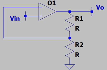
a) 1 + (R2/R1)
b) 1 + R1
c) 1 + R2
d) 1 + (R1/R2)
View Answer
Explanation: This is the basic non-inverting amplifier with a voltage gain of 1 + (R1/R2). Note that since the OPAMP is ideal, the expression of voltage gain is very simple and it gets more complicated for practical OMAMPs.
2. What is the voltage gain of the following circuit? Assume that the B.J.T. has early effect and is biased at a fixed operating point while the OPAMP is ideal.
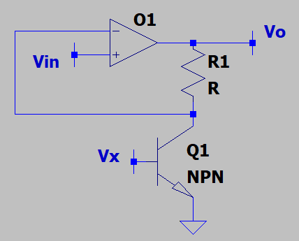
a) 1 + 2*R1
b) 1 + ro1
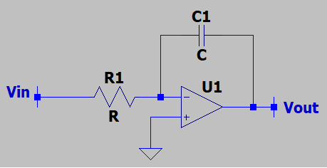
c) 1 + (R1/ro1)
d) 1 + 2*(R1/ro1)
View Answer
Explanation: We note that the output impedance of the npn transistor at the collector end is ro1=IC/VA. Henceforth, since the transistor is biased at a constant voltage, which means a constant IC, the output resistance is constant and the voltage gain of the opamp is 1 + (R1/ro1).
3. What is the voltage gain of the following circuit? Assume that the B.J.T. is ideal, biased at a fixed operating point, while the OPAMP is ideal.
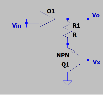
a) 1 + (3*R1)
b) 1 + (R1*gm)
c) 1 + R1/gm
d) 1 + 6(R1*gm)
View Answer
Explanation: We note that the output impedance of the npn transistor at the emitter end is 1/gm=VT/IC. Henceforth, since the transistor is biased at a constant voltage, which means a constant IC, the output resistance is constant and the voltage gain of the opamp is 1 + (R1*gm). Note that we need to find a suitable VX to ensure that the transistor remains in the active region.
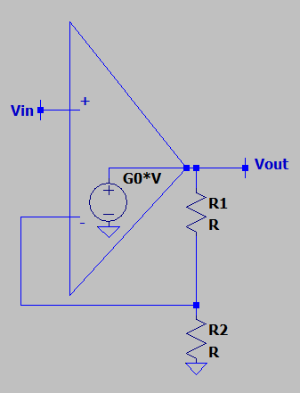
4. If we assume that the OPAMP has a finite, but very high, voltage gain, say G0, what is the voltage gain for the following circuit?
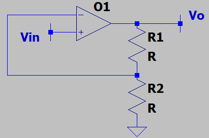
a) \(\frac {1}{((\frac {1}{G_0})+R_2)}\)
b) \(\frac {1}{((\frac {1}{G_0})+(R_1 + R_2))}\)
c) \(\frac {1}{((\frac {1}{G_0})+\frac {R_1}{(R_1+R_2)})}\)
d) \(\frac {1}{((\frac {1}{G_0})+\frac {R_2}{(R_1+R_2)})}\)
View Answer
Explanation: Since the OPAMP has a finite voltage gain, we use the model of the OPAMP as shown below where V is the difference between the two input voltages. Henceforth, we solve the circuit to get the voltage gain as \(\frac {1}{((\frac {1}{G_0})+\frac {R_2}{(R_1+R_2)})}\). Note that the expression reduces to (1 + (R1/R2)) as G0 tends to infinity.
5. If we assume that the OPAMP has a finite, but very high, voltage gain, say G0, what is the voltage gain for the following circuit? The BJT has early effect but it is biased to a fixed operating point.
a) 1/((1/G0)+1/(R1+ro1))
b) 1/((1/G0)+(R1+ro1))
c) 1/((1/G0)+ro1/(R1+ro1))
d) 1/((1/G0)+ro1))
View Answer
Explanation: Since the OPAMP has a finite voltage gain, we use the model of the OPAMP where V is the difference between the two input voltages. Henceforth, we solve the circuit to get the voltage gain as 1/((1/G0)+ro1/(R1+ro1)), ro1 is the output resistance of the BJT at the collector side. Note that the expression reduces to (1 + (R1/ro1)) as G0 tends to infinity. We will have to be careful when taking deciding the value of VX as it will have a range of values which depends on the range of the input voltage, so that the BJT remains in the active region.
6. If we assume that the OPAMP has a finite, but very high, voltage gain, say G0, what is the voltage gain for the following circuit? The BJT has early effect but it is biased to a fixed operating point.
a) 1/((1/G0)+1/gm1/(R1+1/gm1))
b) 1/((1/G0)+1/gm1))
c) 1/((1/G0)+1/gm1/(R1))
d) 1/((1/G0)+(R1+1/gm1))
View Answer
Explanation: As the OPAMP has a finite voltage gain, we use the model of the OPAMP and we solve the circuit to get the voltage gain as
1/((1/G0)+1/gm1/(R1+1/gm1)), 1/gm1 is the output resistance of the BJT at the emitter side. Note that the expression reduces to (1 + (R1*gm1)) as G0 tends to infinity.
7. In the following circuit, the OPAMP is ideal, what is the voltage gain?
a) -R2/R1
b) -R2/R1
c) -R2/R1
d) Infinite
View Answer
Explanation: This is the basic inverting amplifier configuration, using the OPAMP. The voltage gain is simply -R2/R1 and we need to consider that the inverting node is shorted to a virtual ground.
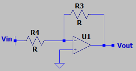
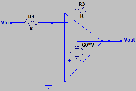
8. In the following circuit, the OPAMP is non-ideal, what is the voltage gain?
a) -1/((R1+R2)/R1)+R2/R1)
b) -1/(1/G0(R1))+R2/R1)
c) -1/(1/G0(R1+R2)/R1))
d) -1/(1/G0(R3+R4)/R3)+R4/R3)
View Answer
Explanation: The non-ideal OPAMP has a finite voltage gain and we use the model to calculate the voltage gain. After solving the circuit, it comes out to be -1/(1/G0(R3+R4)/R3)+R4/R3). Note that the gain becomes -R3/R4 as G0 goes to infinity.
9. What is the voltage gain of the following circuit? Assume that the BJT and OPAMP is ideal, the BJT is working in the active region.
a) [(R4+R5)/R3]*(R5||R4)
b) [(R4+R5)/R3]*gm
c) [(R4+R5)/R3]*gm*(R5||R4)]
d) -[(R4+R5)/R3]*gm*(R5||R4)]
View Answer
Explanation: The total resistance connected to the collector is R5 & R4, the virtual ground at the negative terminal will eliminate the effect of R3. This voltage gain gets multiplied with the gain of the OPAMP which is -(R4+R5)/R3, note that the resistance looking away from the negative terminal towards R4 is (R4+R5) as the BJT offers infinite output impedance ideally. The overall gain is [(R4+R5)/R3]*gm*(R5||R4)].
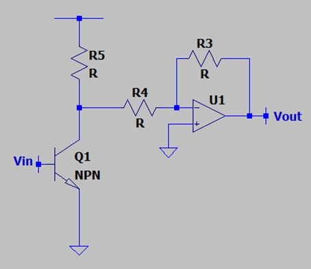
10. What is the voltage gain of the following circuit if the OPAMP is non-ideal? Assume that the BJT is ideal and biased to operate in the active region.
a) [1/(1/G0*R3)+(R4+R5)/R3)]*gm*(R5||R4)
b) -[1/(1/G0)+(R4+R5)/R3)]*gm*(R5||R4)
c) [1/(1/G0(R3+(R4+R5))/R3)+(R4+R5)/R3)]*gm*(R5||R4)
d) -[1/((R3+(R4+R5))/R3)+(R4+R5)/R3)]*gm*(R5||R4)
View Answer
Explanation: The voltage gain for the CE stage becomes -gm*(R5||R4). The gain of the offered by the OPAMP in the inverting amplifier configuration is -1/(1/G0(R3+(R4+R5))/R3)+(R4+R5)/R3). The total voltage gain becomes [1/(1/G0(R3+(R4+R5))/R3)+(R4+R5)/R3)]*gm*(R5||R4).
11. What is the voltage gain of the following circuit, if the OPAMP is ideal?
a) t/2R1C1
b) -t/R1C1
c) t/R1C1
d) -t/C1
View Answer
Explanation: This is the basic Integrator circuit. In the s domain, the voltage gain is simply -t/sR1C1 & if we take the inverse Laplace transform, the voltage gain becomes -t/R1C1.
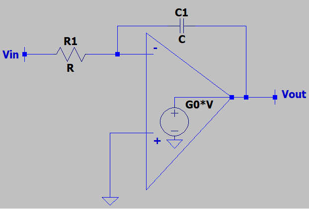
12. If the OPAMP in the following circuit is non-ideal, what is the voltage gain of the following circuit?
a) 1/(1/G0*(1+1/A0))
b) 1/(1/G0+(R1C1s)(1+1/A0))
c) 1/(1/G0+(R1C1s))
d) 1/(R1C1s)(1+1/A0))
View Answer
Explanation: We use the model of the OPAMP and we will solve the circuit using a nodal analysis at the inverting terminal and then the rest is algebraic manipulation. The overall voltage gain is -1/(1/G0+(R1C1s)(1+1/A0)). Note that as G0 tends to infinity, the voltage gain again becomes -1/R1C1s.
13. What is the -3dB pole frequency of the following circuit if the OPAMP has a finite gain?
a) -1/R1C1(1+2*G0)
b) -1/R1(1+G0)
c) -1/C1(1+G0)
d) -1/R1C1(1+G0)
View Answer
Explanation: In presence of a finite gain, the voltage gain is -1/(1/G0+(R1C1s)(1+1/A0)). The pole frequency is the frequency when the voltage gain starts to roll of as the input frequency becomes comparable to the pole frequency and this is found by setting the denominator to 0. Henceforth, the -3dB pole frequency becomes -1/R1C1(1+G0).
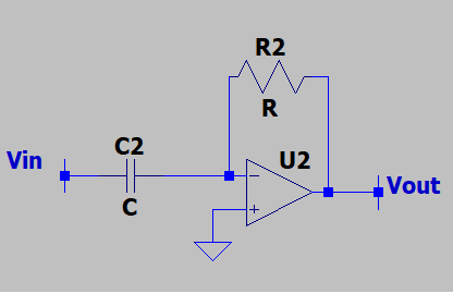
14. What is the voltage gain of the following circuit? Assume that the OPAMP is ideal.
a) R1C1s
b) -R1C1s
c) -C1s
d) -R1s
View Answer
Explanation: This is the basic differentiator circuit. The voltage gain is given by -R1C1s and the time domain response is obtained by taking the inverse Laplace transform which readily shows the differentiation property of this circuit.
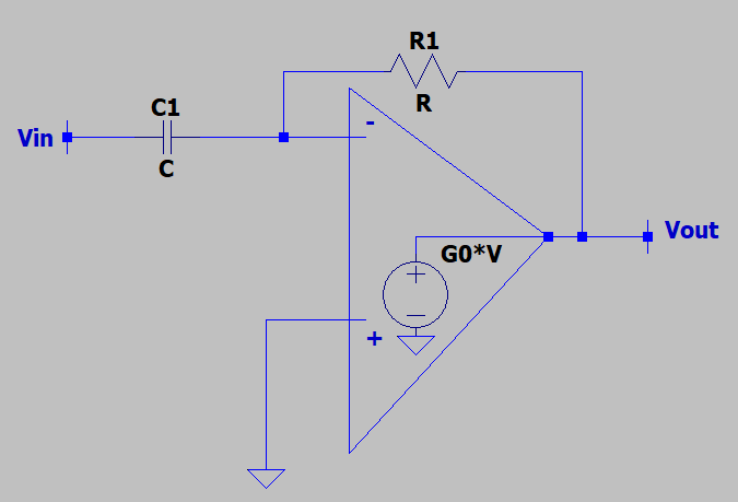
15. What is the voltage gain of the following circuit? Assume that the OPAMP has a finite voltage gain.
a) R1C1s/(1/G0*(1+R1C1s))
b) -R1C1s/(1/G0*(1+R1C1s)+1)
c) -R1s/(1/G0*(1+R1C1s))
d) -C1s/(1/G0*(1+R1C1s+1)
View Answer
Explanation: Since the OPAMP is non-ideal, it is expected to have a finite voltage gain. So, we need to use the model of the OPAMP and solve for the gain. We will only have to write a KCL at the inverting terminal and solve for VOUT and the voltage gain is given by -R1C1s/(1/G0*(1+R1C1s)+1). Note that the gain becomes -R1C1s as G0 tends to infinity.
Sanfoundry Global Education & Learning Series – Microelectronics.
To practice all areas of Microelectronics, here is complete set of 1000+ Multiple Choice Questions and Answers.
If you find a mistake in question / option / answer, kindly take a screenshot and email to [email protected]
