This set of Microelectronics Multiple Choice Questions & Answers (MCQs) focuses on “Low Frequency Response of Stages of BJT”.
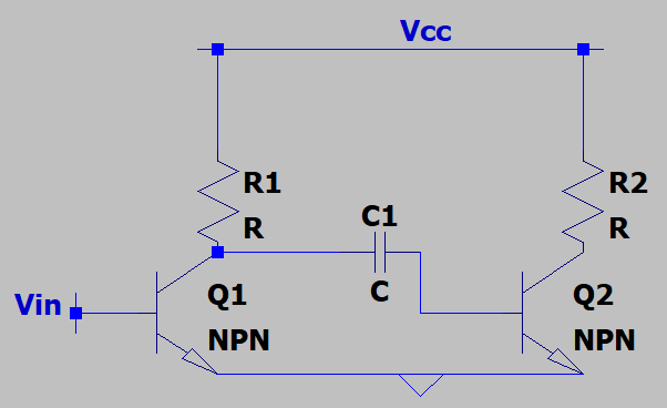
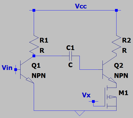
1. The frequency of the input voltage is Ω. What is the input impedance of Q2 which allows us to decide a value for C1 such that the impedance of C1 is less than the input impedance at the frequency of interest?
a) rπ
b) rπ+R
c) rπ-R
d) Infinite
View Answer
Explanation: The coupling capacitor has to behave like a short circuit at frequencies of interest. The impedance of the coupling capacitor is 1/CΩ & this should be less than the input impedance of the Q2, which is simply rπ.
2. The frequency of the input voltage is Ω. What is the input impedance of Q2 which allows us to decide a value for C1 such that the impedance of C1 is less than the input impedance at the frequency of interest?
a) (β+1)R
b) rπ+(β+1)R
c) rπ-(β+1)R
d) Infinite
View Answer
Explanation: Q2 is degenerated by a resistance of R. This will increase it’s input impedance by an amount (β+1)*R where β is the current gain.
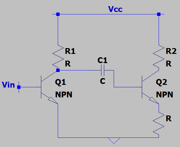
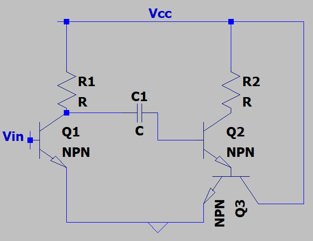
3. The frequency of the input voltage is Ω. What is the input impedance of Q2 which allows us to decide a value for C1 such that the impedance of C1 is less than the input impedance at the frequency of interest?
a) (β+1)R
b) rπ+(β+1)ro3
c) rπ-(β-1)ro2
d) Infinite
View Answer
Explanation: Q2 is degenerated by the output impedance of Q3. This will increase it’s input impedance by an amount (β+1)*(ro3) where β is the current gain. Note that ro3 is assumed to be held at a value by a constant bias.
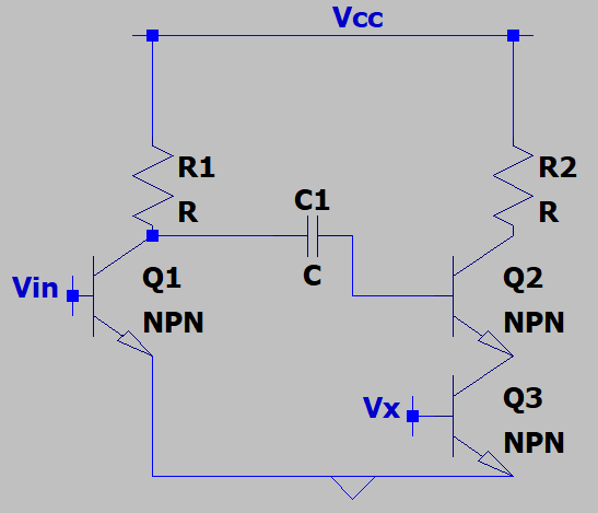
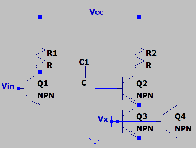
4. The frequency of the input voltage is Ω. What is the input impedance of Q2 which allows us to decide a value for C1 such that the impedance of C1 is less than the input impedance at the frequency of interest?
a) (β+1)ro3
b) rπ+(β-1)(ro3||ro4)
c) rπ-(β-1)ro2
d) rπ+(β+1)(ro3||ro4)
View Answer
Explanation: Q2 is degenerated by the output impedance of Q3 & Q4. This will increase it’s input impedance by an amount (β+1)*(ro3||ro4) where β is the current gain. Note that ro3 & ro4 is assumed to be held at a value by a constant bias.
5. If C1 is assumed to be a short circuit at a certain frequency, in an ideal situation, what is the small signal voltage gain of Q1?
a) -gm*(R1||(rπ-(β+1)R))
b) -gm*(R2||(rπ-(β+1)R))
c) -gm*(R1||(rπ+(β+1)R))
d) -gm*(R2||(rπ+(β+1)R))
View Answer
Explanation: Q1 behaves as a C.E. stage. It’s output impedance is (R1||(rπ+(β+1)R). Note that the total resistance for Q2 has increased due to degeneration. The gain becomes -gm*(R1||(rπ+(β+1)R)).
6. If C1 is assumed to be a short circuit at a certain frequency, in an ideal situation, what is the small signal voltage gain of Q1?
a) gm*(R1||(rπ+(β+1)(ro4)))
b) gm*(R1||(rπ+(β+1)(ro3)))
c) -gm*(R1||(rπ+(β+1)(ro3||ro4)))
d) -gm*(R1||(rπ+(β+1)(ro3||ro4))
View Answer
Explanation: Q1 behaves as a C.E. stage. It’s output impedance is (R1||(rπ+(β+1)(ro3||ro4))). Note that the total resistance for Q2 has increased due to degeneration by the two npn transistors. The gain becomes -gm*(R1||(rπ+(β+1)(ro3||ro4))).
7. If C1 is assumed to be a short circuit at a certain frequency, in an ideal situation, what is the small signal voltage gain of Q1?
a) gm*(R1||(rπ+(β*1)(ro2)))
b) gm*(R1||(rπ+(β-1)(ro4)))
c) -gm*(R1||(rπ+(β+1)(ro3||ro4)))
d) -gm*(R1||(rπ+(β+1)(ro1)))
View Answer
Explanation: Q1 behaves as a C.E. stage. It’s output impedance is R1||(rπ+(β+1)(ro1)). The formulae for calculating the output impedance for the MOSFET and the BJT are different. However, the voltage gain becomes -gm*(R1||(rπ+(β+1)(ro1))).
8. The frequency of the input voltage is Ω. What is the input impedance of Q2 which allows us to decide a value for C1 such that the impedance of C1 is less than the input impedance at the frequency of interest?

a) rπ1+(β+1)*(1/gm3)
b) rπ2+(β+1)*(1/gm5)
c) rπ2+(β-1)*(1/gm5)
d) rπ1+(β+1)*(1/gm2)
View Answer
Explanation: Q2 is degenerated by the output impedance of Q5. This will increase it’s input impedance by an amount (β+1)*(1/gm5) where β is the current gain. Note that 1/gm5 is assumed to be held at a value by a constant bias.
9. The frequency of the input voltage is Ω. What is the input impedance of Q2 which allows us to decide a value for C1 such that the impedance of C1 is less than the input impedance at the frequency of interest?
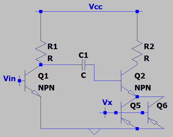
a) rπ2+(β-1)*(1/gm5||1/gm6)
b) rπ2+(β+1)*(1/gm5||1/gm6)
c) rπ2+(β-1)*(1/gm5+1/gm6)
d) rπ2+(β+1)*(1/gm5+1/gm6)
View Answer
Explanation: Q2 is degenerated by the output impedance of Q5. This will increase it’s input impedance by an amount (β+1)*(1/gm5||1/gm6) where β is the current gain. Note that 1/gm5 & 1/gm6 is assumed to be held at a value by a constant bias. The three terminals of each transistor being connected to one another, they are in parallel.
10. What happens to Q5 for a low VIN? Assume that C1 is shorted.
a) High
b) Low
c) Moderately High
d) Moderately Low
View Answer
Explanation: If VIN is low, the input to the base of Q2 is expected to be high if C1 is reasonably short. Thus, the base of Q3 follows the base of Q2 and is expected to be approximately high and the transistor is behaving as a C.E. stage.
11. The frequency of the input voltage is Ω. What is the input impedance of Q2 which allows us to decide a value for C1 such that the impedance of C1 is less than the input impedance at the frequency of interest?
a) rπ2+(β-1)rπ3
b) (β+1)rπ2+rπ3
c) rπ2+rπ3
d) rπ2+(β+1)rπ3
View Answer
Explanation: Q2 is degenerated by the input impedance of Q3. This is simply rπ. The overall input impedance becomes rπ2+(β+1)rπ3.
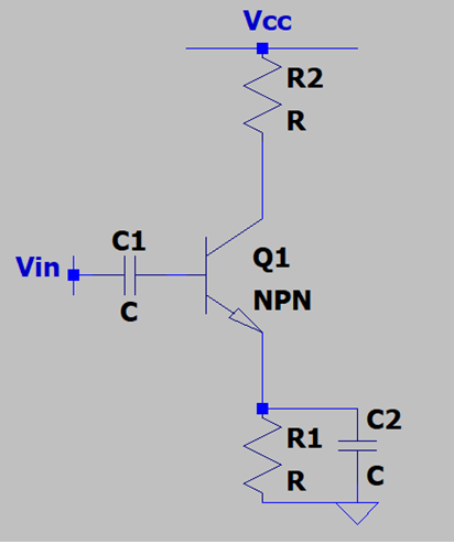
12. If the transconductance of Q1 is provided to be g Siemens, what should be the factor by which the capacitance of the coupling capacitor is related to the inverse of its transconductance such that the input is shorted to the base of the transistor?
a) Capacitance much less than g
b) Capacitance much more than g
c) Capacitance equal to g
d) Frequency of operation not mentioned
View Answer
Explanation: The impedance of the coupling capacitor will have to be less than the input impedance of Q1. The input impedance of Q1 is rπ1.This is inversely proportional to g. The impedance will have to be less than 1/g and hence the capacitance will have to be much less than g. It is to be assumed that C2 shorts R1 to ground and is a bypass capacitor.
13. If the effect of the degenerating resistance is to be reduced, what should be the value of the capacitance such that it gets shorted to ground at low frequencies?
a) less than 1/g
b) greater than 1/g
c) equal to 1/g
d) equal to 2/g
View Answer
Explanation: The effect of the degenerating resistor is to increase the input impedance, we need to make sure that rπ1 dominates the expression of input impedance (β+1)*1/wC2 + rπ and hence (β+1)*1/wC2 < rπ ie less than β/gm.
Sanfoundry Global Education & Learning Series – Microelectronics.
To practice all areas of Microelectronics, here is complete set of 1000+ Multiple Choice Questions and Answers.
If you find a mistake in question / option / answer, kindly take a screenshot and email to [email protected]
